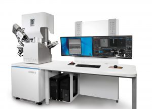
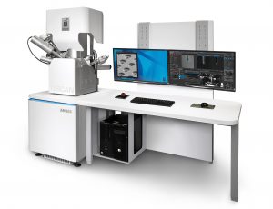
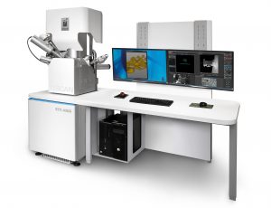
The configuration in FIB-SEM systems is such that the electron and ion beam focal points coincide, which results in the optimisation of many applications. Such a feature enables simultaneous SEM imaging during FIB milling tasks – a significant leap in terms of performance and throughput in all those FIB operations which demand ultimate levels of precision.
TESCAN offers two different ion species as source for FIBs: Gallium ions and Xenon ion plasma. Ga ion source FIB is for all those applications that need ultimate precision in fabrication and nanopatterning. On the other hand, Xe plasma FIBs enable high ion beam currents that make it possible to remove large volumes of material in times frames that can be up to 50 × shorter compared to Ga-FIBs. In terms of precision, our high-resolution Xe plasma FIBs can achieve resolution of < 15 nm for all those delicate tasks that need power and precision combined.
Our wide range of FIB-SEM systems are aimed to satisfy from basic industrial routine applications to the most advanced and challenging technological applications that demand the highest standards in imaging and micro/nanomachining for their complex workflows.
TESCAN FIB-SEM Solutions for Materials Science
Focus Ion Beam Scanning Electron Microscopy (FIB-SEM) has become an essential tool for materials science and engineering. TESCAN offers an extended portfolio of turnkey systems, tailored to help scientists and researchers in materials science make progress and achieve their goals. TESCAN’s broad range of dedicated and innovative instruments is part of our firm commitment to push materials science forward.
TESCAN FIB-SEM Solutions for Life Sciences
TESCAN world-class imaging technology delivers complete solutions for researchers in all branches of science. No matter what sample type and size, and what questions are being asked, there is always a dedicated solution available to solve all required tasks. Due to the high versatility and customizable design of all TESCAN systems, it is very easy to design and manufacture dedicated instruments suited exactly to the customer’s needs. The available instrumentation encompasses ultrahigh-resolution imaging, variable pressure observations, 3D tomographic methods, and complex solutions including correlative light-electron microscopy or cryogenic techniques.
TESCAN FIB-SEM Solutions for Semiconductors
The semiconductor industry is engaged in a relentless race where the aim is high integration, high density and miniaturisation of logic devices. This has resulted in the development of new technologies such as 3D ICs that make it possible to integrate extensive functionality into ever smaller, faster and lower power consumption devices. However, these more complicated integrated circuits require more sophisticated tools for development and prototyping, inspection and failure analysis in order to analyse or reach the areas of interest.


